A TPU is fundamentally a matrix multiply engine (MXU) bolted to a stack of fast memory (HBM), with a small scratchpad (VMEM) sitting between them.
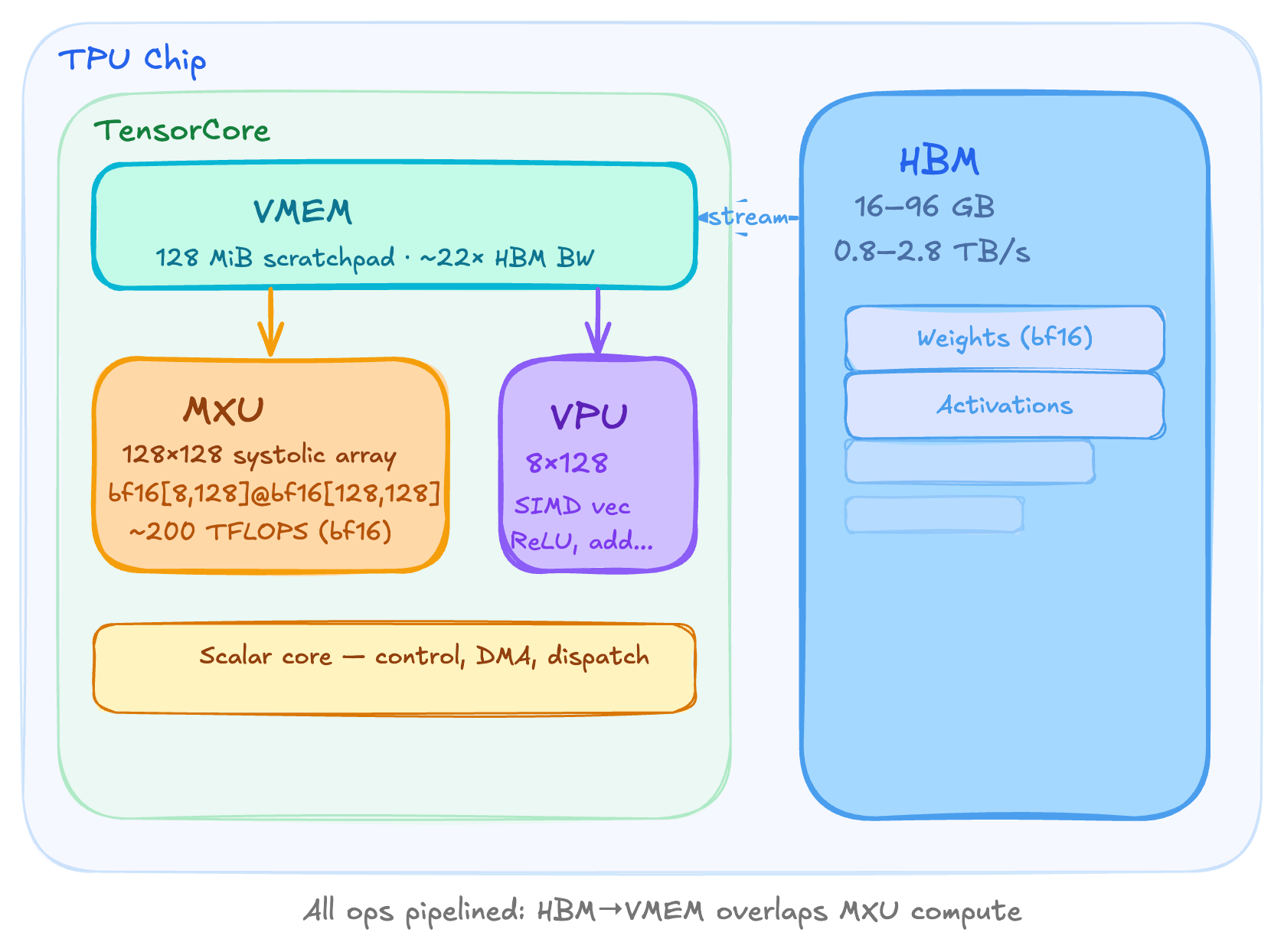
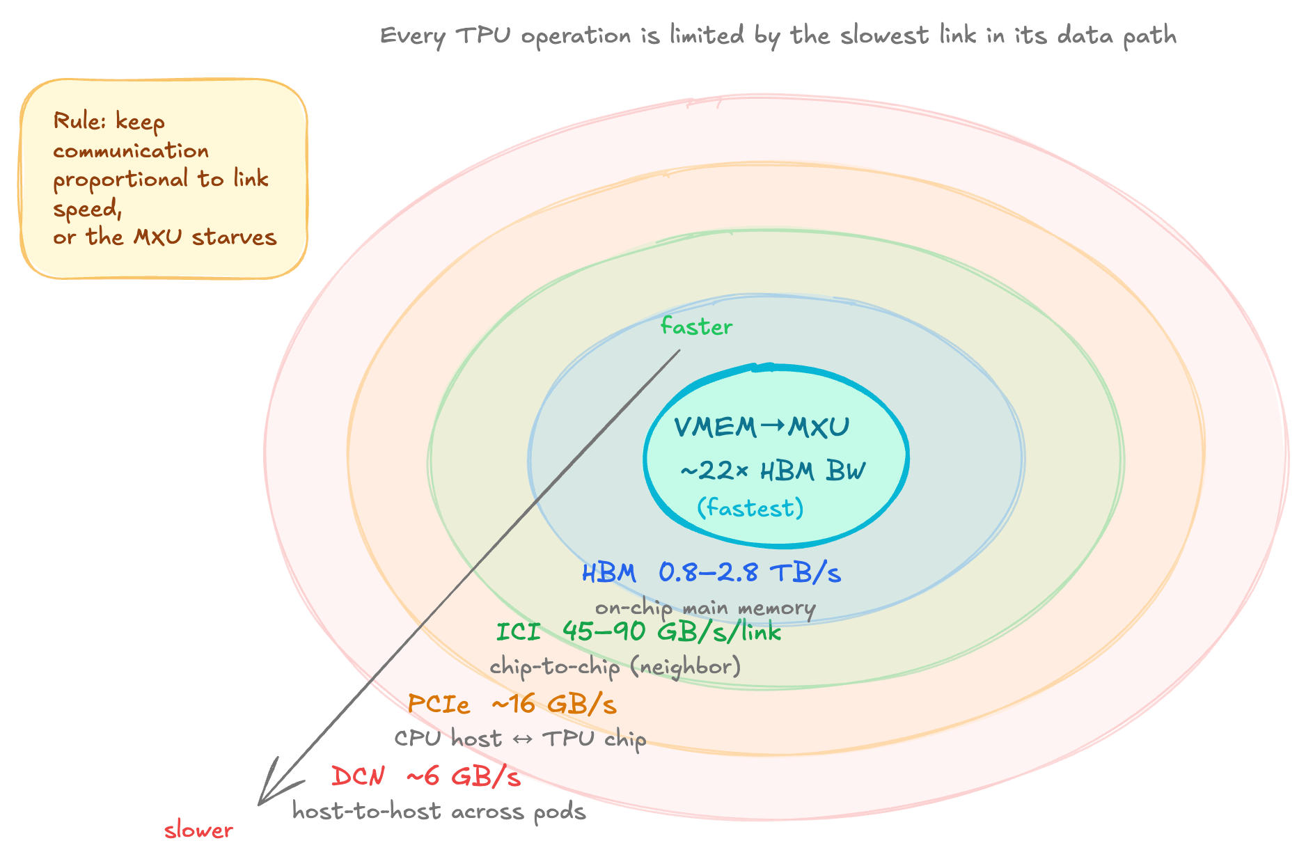
HBM (high bandwidth memory) is the main storage on a TPU chip. It holds all your weights, activations, KV caches etc. Its capacity ranges from 16 GB on v5e to 96 GB on v5p. The bandwidth between HBM and the tensor core is typically 0.8 to 2.8 TB/s. This bandwidth is the single most important bottleneck for memory-bound workloads like LLM inference at small batch sizes. When people say we are bandwidth-bound, they almost always mean this limit.
VMEM is an on-chip scratchpad sitting inside the denser core and it's very physically close to the compute units. It's much smaller than HBM but has roughly 22× higher bandwidth to the MXU. The data in HBM must be copied into VMEM before the MXU can touch it. This huge bandwidth advantage means that if you can fit your operands in VMEM, the arithmetic intensity threshold to stay compute bound drops from 240 to 11.
The MXU is the heart of the TPU. It's a 128×128 systolic array (or 256×256 on v6e) that performs one bf16[8,128]×bf16[128,128]→f32[8,128] matmul every 8 clock cycles. The reason TPUs are so efficient at MatMuls is because matrix multiplication is O(n3) on compute, while being O(n2) in data. A well-designed arithmetic unit is truly going to be compute-bound rather than memory-bound.
The VPU handles everything that is not matrix multiplication. This includes activation functions, softmax, layer norm, point-wise operations and reductions. It's a SIMD machine and it is about 10× slower than the MXU in raw throughput. This is intentional because in a transformer, matrix multiplications dominate the total FLOPs, so the silicon budget is allocated accordingly.
Finally, the scalar core dispatches instructions, manages DMA transfers, and handles control flow. It is single-threaded, which limits the TPU to one DMA request per cycle.
Pipelining is useful
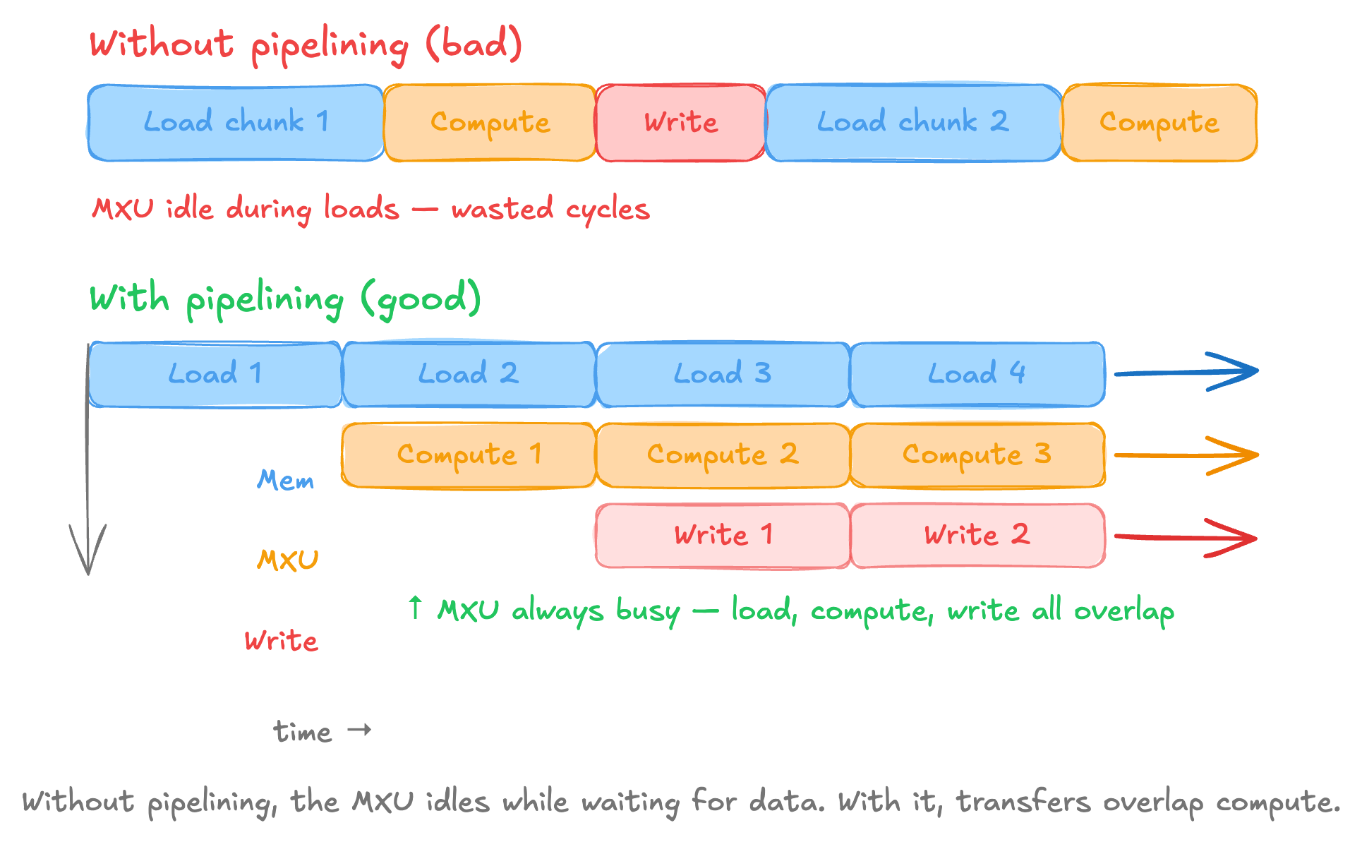
Pipelining overlaps the stages of loading weights, activations from HBM then computing in MXU and then writing the results back to the HBM so they can happen concurrently.
Without pipelining, the MXU will have to be idle during loads and this is incredibly wasteful. The concept of pipelining is analogous to CPU instruction pipelining, but at a much
coarser granularity where each stage in the pipeline moves megabytes not bytes.
In practice, the TPU chunks a large matmul into tiles.
While the MXU multiplies tile N, the DMA engine is loading tile N+1 from HBM into VMEM and writing tile N-1's results from VMEM back to HBM.
If the HBM to VMEM transfer for each tile takes longer than the MXU compute for that tile, the MXU finishes and has nothing to do until the next tile arrives.
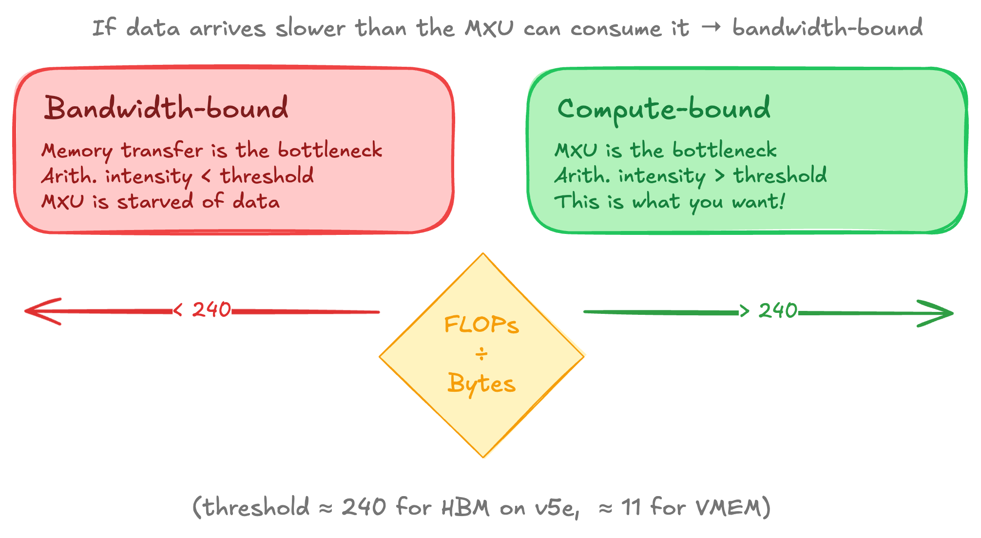
You are now bandwidth-bound. The crossover point is the arithmetic intensity threshold.
Arithmetic intensity of a computation is the ratio of FLOPs performed and bytes transferred. For a matmul bf16[B,D]×bf16[D,F], you do 2BDF FLOPs and transfer 2(BD+DF+BF) bytes. On v5e, the HBM roofline threshold is FLOPs/s÷HBM_BW=1.97×1014/8.1×1011≈240. If your operation's arithmetic intensity exceeds 240, you're compute-bound (good). Below that, you're bandwidth-bound (the MXU is underutilized).
For VMEM, the threshold drops to about 11 because VMEM bandwidth is about 22× higher. This makes fitting operands in VMEM powerful since small batch sizes are enough to make the workload compute bound that would otherwise be bandwidth bound over HBM.
The compute bound vs bandwidth bound distinction is crucial for performance reasoning. Pretty much every optimization strategy such as batching, quantization, sharding, prefetching ultimately aims to push your workfload into the compute bound regime.
Here is a relevant post I made on calculating rooflines.
What makes up a SuperPod?
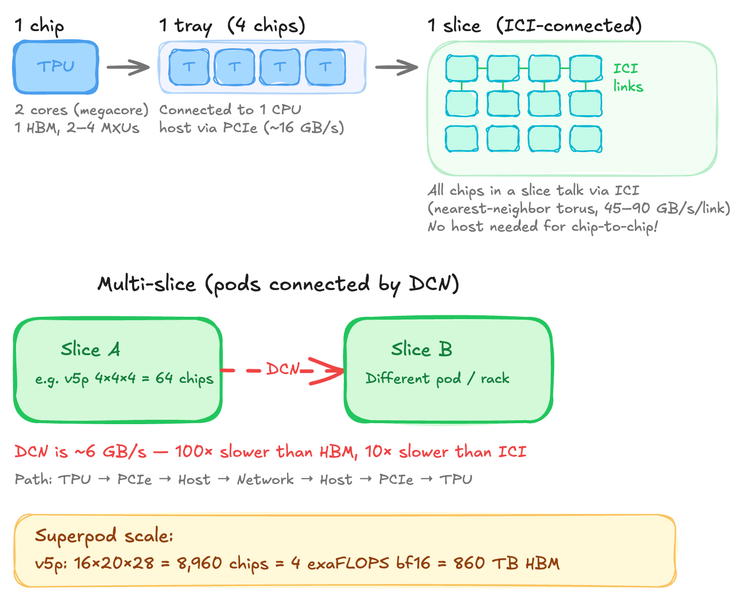
A chip is a single TPU die. Since v4, most chips have two TensorCores sharing HBM in a "megacore" configuration where they appear as one logical accelerator with double the FLOPs (v5e is an exception with 1 core per chip).
A tray is 4 chips connected to a single CPU host via PCIe. This is typically what we get in Colab or a single TPU-VM. The host provides CPU RAM, networking and manages I/O.
A slice is a set of ICI-connected chops forming a torus. This is where the interesting topology lives. v5e/v6e form a 2D torus whereas a v4p/v5p forms a 3D torus. Within a slice, chips communicate directly over ICI without host involvment. The torus topology is key since it wraps edges around so the max distance between any two nodes is N/2 instead of N.
Wraparound links only exist on axes of size 16 or multiples of 4. For example, a 2x2x4 slice has no wraparounds whereas a 4x4x4 slice has. Without wraparounds maximum hop distance doubles and bidirectional ring bandwidth halves.
A pod or superpod are slices connected by DCN. The DCN path is expensive. To send data from a TPU on slice A to a TPU on slice B, the path is TPU -> PCIe -> Host A -> DCN -> Host B -> PCIe -> TPU.
The Five Characteristic Speeds of TPU
This is a good model of hierarchy to have when reasoning about TPU performance.
-
VMEM → MXU. The VMEM is on-chip and is effectively free. If the data is already in VMEM, the MXU can consume it at full speed. The bottleneck is VMEM's tiny size (~128MB) so only small weight tiles or heavily sharded layers fit.
-
HBM ↔ VMEM. This is the primary bottleneck for most single-chip workloads. The ratio of MXU FLOPs to HBM bandwidth gives you the roofline arithmetic intensity (~240 for v5e, 160 for v4p, etc)
-
ICI (Inter-chip Interconnect). This is used for communication within a slice. This is the bottleneck when you shard models across chips. ICI links connect nearest neighbors, so data travelling to distant chips must hop through intermediate ones. A v5p chip has 3 ICI axes (6 links), while v5e/v6e have 2 axes (4 links).
TPU vs GPU Networking
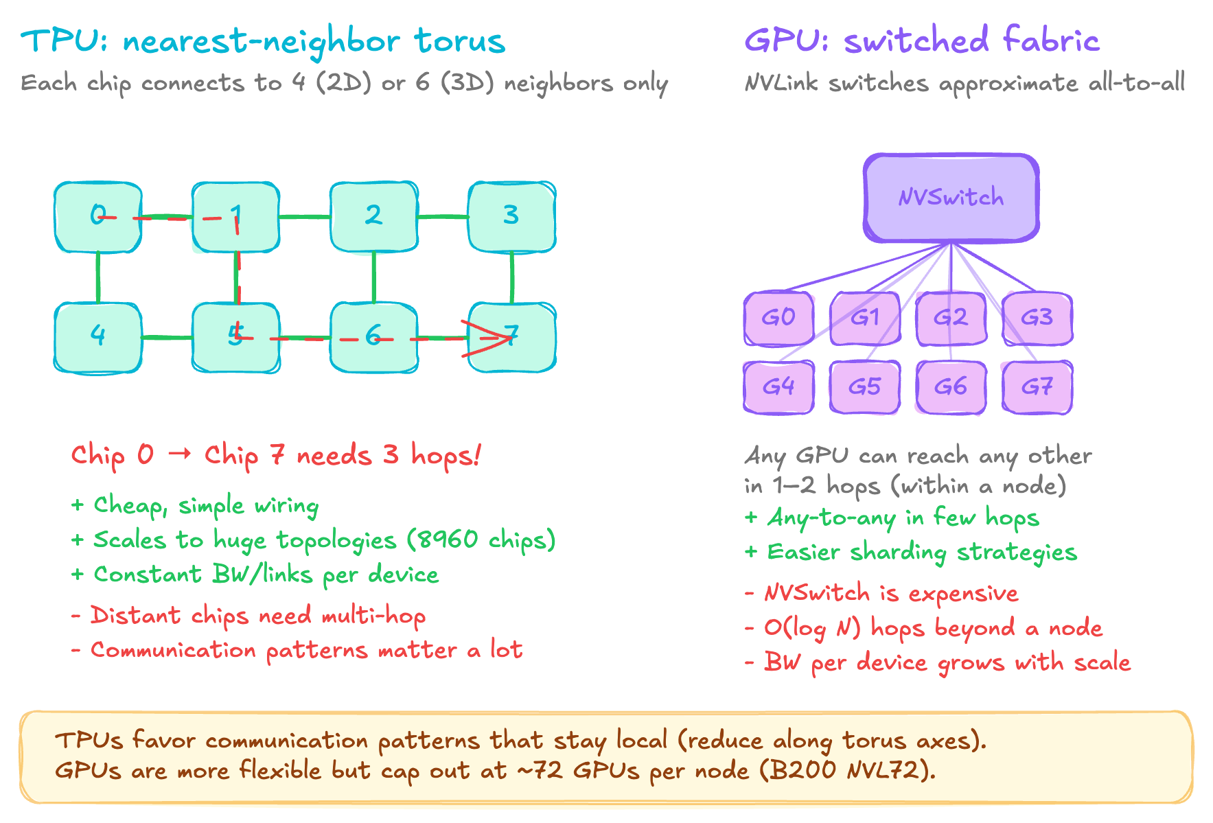
The TPU approach is nearest-neighbor torus where each chip has 4 (2D) or 6 (3D) direct links to adjacent chips. To reach a distant chip data hops through every intervening chip. The benefits are that wiring is simple and link count per chip is constant regardless of what the cluster size is, and you can scale to enormous topologies because you don't need expensive switch infrastructure. The trade-off is that communication patterns must respect this locality. For example, an all-reduce along a torus axis is efficient because it can use a ring-based algorithm, but arbitrary point-to-point communication between distant chips will incur multi-hop latency.
The GPU approach is to use the switched fabric of NVLink + NVSwitch. Within a node, let's say 8 GPUs for H100 or 72 for B200 NVL72, GPUs are connected through NVSwitch, which approximates all-to-all connectivity. Any GPU can reach any other in one or two hops and beyond a node InfiniiBand or NVLink network provides a O(logN) connectivity through a fat tree switch topology. The upside is that the communication patterns can be more flexible and the programming model is simpler, but the trade-off is that NVSwitch is expensive silicon and switch hierarchy adds cost and complexity, and scaling beyond a node requires a separate network fabric.
So practically, on TPUs you want to shard along the torus axis and use ring-based collectives like all-reduce and all-gather that naturally map to the torus. Communication that crosses many hops, like gathering from all chips to one, is expensive. The interconnect bandwidth is symmetric because every chip has the same number of links and load balancing is natural, but you must respect the topology.
Estimating Inference Latency and Potential Optimizations
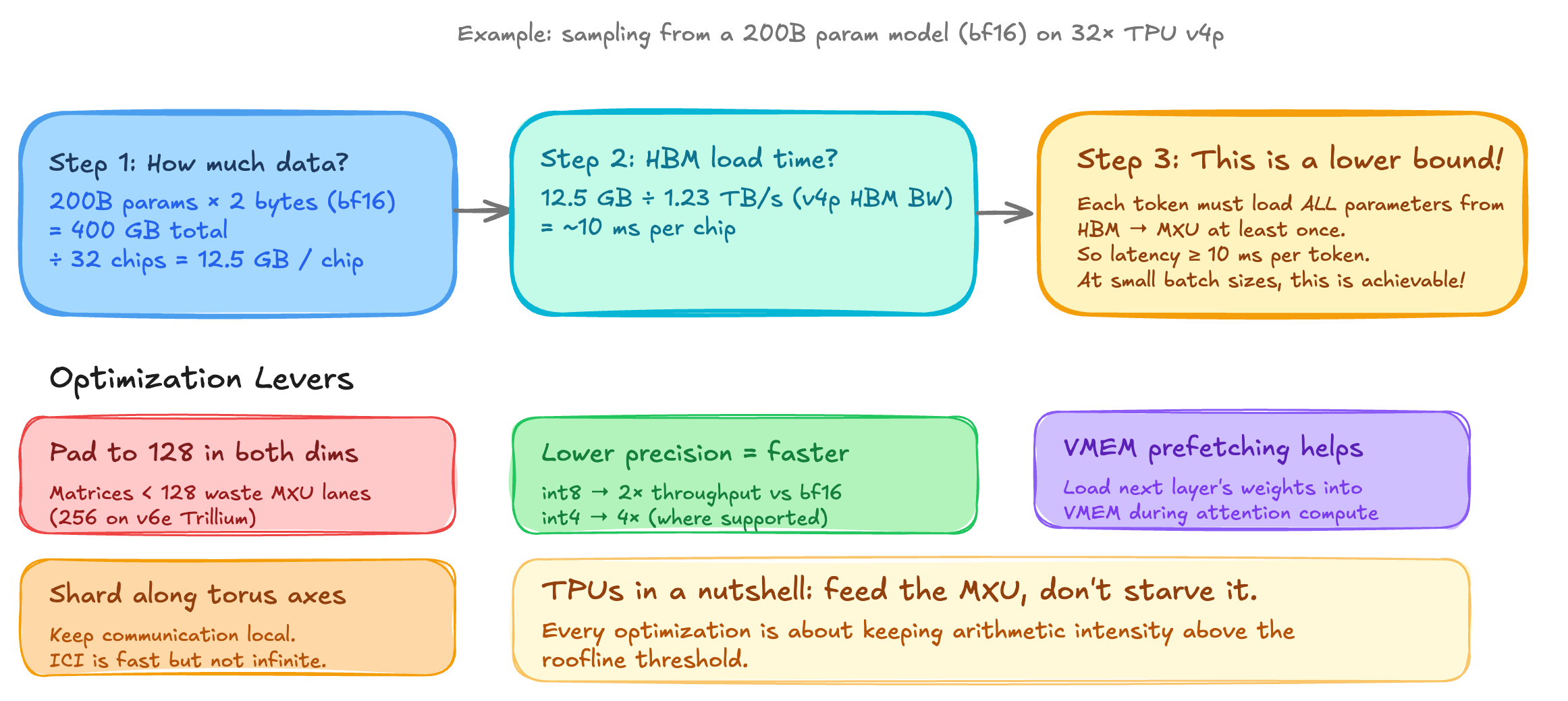
Let's walk through an example. Suppose we want to sample from a 200B parameter model in BF16 on 32 TPU V4P chips. The total weights are 200 x 10^9 x 2 bytes = 400 GB. That's 12.5 GB per chip and with each chip at 1.23 TB/s HBM bandwidth loading weights across the 32 chips takes ~10 ms. Since every autoregressive decoding step requires loading all parameters at least once from the HBM through the MXU, 10 ms is a hard lower bound on per-token latency.
Here are four optimization levers that you can rely on:
- Pad to 128. The MXU is a 128 by 128 grid. If your matrix has dimensions 100, it gets padded to 128, wasting ~22% of the compute. If it's 129, it gets padded to 256, wasting 50%, so always size your model dimensions as multiples of 128.
- Lower precision. TPUs can do iny8 at 2x the BF16 throughput and, int4, at 4x the throughput. This directly doubles or quadruples your effective flops ceiling, and the roofline threshold also changes because you're moving fewer bytes. Per-parameter quantization is one of the most effective signal optimizations for inference.
- VMEM prefetching. In a standard transformer forward pass, you compute attention, which is relatively small in weights, and then feed forward, which is large. If the feed forward weights are small enough to fit in VMEM you can preload them during the tension. This helps hide the HBM to VMEM transfer cost for the feed forward layer, effectively making it free from a bandwidth perspective.
- Shard along torus axis. In a splitted model across chips, the collective communication should flow along the ICI torus rings. This uses the fast ICI bandwidth rather than the slow PCIe or the DCN path.
Reference: TPUs — Scaling Book (JAX ML). Most of the numbers and architectural details in this post are sourced from or cross-checked against this reference.